- 您现在的位置:买卖IC网 > Sheet目录341 > MAX8831EWE+T (Maxim Integrated)IC LED DRIVR WHITE BCKLGT 16-WLP
�� �
�
�High-Efficiency,� White� LED� Step-Up� Converter�
�with� I� 2� C� Interface� in� 2mm� x� 2mm� WLP�
�The� typical� value� for� the� input� capacitor� is� 1μF,� and� the�
�typical� value� for� the� output� capacitor� is� 1μF.� Higher�
�value� capacitors� can� reduce� input� and� output� ripple,�
�but� at� the� expense� of� size� and� higher� cost.�
�not� returning� to� minimum� current� before� turning� off� dur-�
�ing� the� blink� OFF� time.� The� blink� ON� and� blink� OFF�
�timers� (t� ON_BLINK� and� t� OFF_BLINK� )� are� programmed�
�according� to� the� following� equations� as� guidance:�
�Diode� Selection�
�The� high� switching� frequency� of� the� MAX8831�
�demands� a� high-speed� rectification� diode� for� optimum�
�t� ON� _� BLINK� ≥�
�t� LED� _� RU�
�32�
�(� LED� _� CODE� +� 1� )�
�efficiency.� A� Schottky� diode� is� recommended� due� to� its�
�fast� recovery� time� and� low� forward� voltage� drop.�
�Ensure� that� the� diode’s� average� and� peak� current� rat-�
�t� OFF� _� BLINK� ≥�
�t� LED� _� RD�
�32�
�(� LED� _� CODE� +� 1� )�
�ing� exceeds� the� average� output� current� and� peak�
�inductor� current.� In� addition,� the� diode’s� reverse� break-�
�down� voltage� must� exceed� V� OUT� .�
�Compensation� Network� Selection�
�The� step-up� converter� is� compensated� for� stability�
�through� an� external� compensation� network� from� COMP�
�to� GND.� The� compensation� capacitor� is� typically�
�0.22μF� for� most� applications.� Note� that� higher� C� COMP�
�values� increase� soft-start� duration,� as� well� as� the� time�
�delay� between� enabling� the� step-up� converter� to� initiat-�
�ing� soft-start.�
�Combining� BLINK� Timer�
�and� RAMP� Functions�
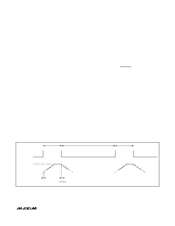
�When� using� the� ramp� functionality� of� LED3,� LED4,� and�
�LED5� in� combination� with� the� blink� timer,� it� is� recom-�
�mended� to� keep� the� ramp-up� timer� shorter� than� the�
�blink� ON� timer� and� the� ramp-down� timer� shorter� than�
�the� blink� OFF� timer.� See� Figure� 14.� Failing� to� comply�
�with� this� restriction� results� in� LED_� current� not� reaching�
�maximum� value� during� blink� ON� time,� and� LED_� current�
�Where� t� LED_RU� is� the� LED_� ramp-up� time,� t� LED_RD� is�
�the� LED_� ramp-down� time,� and� LED_CODE� is� the� deci-�
�mal� equivalent� of� the� ILED_CNTL� register� value� of�
�Table� 2.�
�Using� the� LED3,� LED4,� and� LED5�
�BOOST_CNTRL� Bit�
�The� default� setting� of� the� BOOST_CNTL� bits� (low)�
�include� the� LED3,� LED4,� and� LED5� current� regulators�
�in� the� step-up� converter� minimum� voltage� select� feed-�
�back� circuit.� This� is� intended� for� multi-LED� strings� pow-�
�ered� from� the� step-up� converter.� For� single� LED�
�indicator� lights,� set� the� respective� BOOST_CNTL� bit�
�high,� connect� the� LED� anode� to� the� battery� or� other�
�voltage� source,� and� connect� the� LED� cathode� to� the�
�respective� LED_� input.� Ensure� the� voltage� source� is�
�high� enough� to� satisfy� VF� of� the� LED� plus� 150mV� (cur-�
�rent� regulator� dropout� voltage).� If� BOOST_CNTL� bits�
�are� set� to� high� for� LED3,� LED4,� and� LED5� and� LED1�
�and� LED2� are� not� enabled,� the� step-up� converter� does�
�not� turn� on� when� LED3,� LED4,� or� LED5� is� enabled.�
�BLINK� TIMERS�
�I� LED� =� ILED_CNTL�
�REGISTER� SETTING�
�I� LED_� =� OFF�
�t� ON_BLINK�
�t� OFF_BLINK�
�t� ON_BLINK�
�t=�
�t� LED_RU�
�32�
�t=�
�t� LED_RU�
�32�
�Figure� 14.� Combined� Timing� Characteristics� of� RAMP� and� BLINK� Timers�
�______________________________________________________________________________________�
�19�
�发布紧急采购,3分钟左右您将得到回复。
相关PDF资料
MAX8834ZEWP+T
IC LED DRIVR BCKLGT FLASH 20-WLP
MAX8855EVKIT+
KIT EVAL FOR MAX8855
MAX8879ETG+T
IC LED DRVR WT/RGB BCKLGT 24TQFN
MAX8901BETA+TCH8
IC LED DRIVER WHITE BCKLGT 8TDFN
MAX8930EWJ+T
IC LED DRVR WT/RGB BCKLGT 49WLP
MAXQ2000-KIT
EVAL KIT FOR MAXQ2000
MAXQ610-KIT#
EVALUATION KIT FOR MAXQ610
MB2146-401-01A
KIT STARTER F2MC-8FX 3V
相关代理商/技术参数
MAX8833ETJ+
功能描述:直流/直流开关调节器 Dual 3A 2MHz Step-Down Regulator RoHS:否 制造商:International Rectifier 最大输入电压:21 V 开关频率:1.5 MHz 输出电压:0.5 V to 0.86 V 输出电流:4 A 输出端数量: 最大工作温度: 安装风格:SMD/SMT 封装 / 箱体:PQFN 4 x 5
MAX8833ETJ+T
功能描述:直流/直流开关调节器 Dual 3A 2MHz Step-Down Regulator RoHS:否 制造商:International Rectifier 最大输入电压:21 V 开关频率:1.5 MHz 输出电压:0.5 V to 0.86 V 输出电流:4 A 输出端数量: 最大工作温度: 安装风格:SMD/SMT 封装 / 箱体:PQFN 4 x 5
MAX8834YEVKIT+
功能描述:LED 照明开发工具 Adaptive Step-Up Converters with 1.5A Flash Driver RoHS:否 制造商:Fairchild Semiconductor 产品:Evaluation Kits 用于:FL7732 核心: 电源电压:120V 系列: 封装:
MAX8834YEWP+T
功能描述:LED照明驱动器 Adaptive Step-Up Converter RoHS:否 制造商:STMicroelectronics 输入电压:11.5 V to 23 V 工作频率: 最大电源电流:1.7 mA 输出电流: 最大工作温度: 安装风格:SMD/SMT 封装 / 箱体:SO-16N
MAX8834ZEWP+T
功能描述:LED照明驱动器 Adaptive Step-Up Converter RoHS:否 制造商:STMicroelectronics 输入电压:11.5 V to 23 V 工作频率: 最大电源电流:1.7 mA 输出电流: 最大工作温度: 安装风格:SMD/SMT 封装 / 箱体:SO-16N
MAX8836ZEREEE+T
功能描述:电流型 PWM 控制器 1.2A PWM Step-Down Converter RoHS:否 制造商:Texas Instruments 开关频率:27 KHz 上升时间: 下降时间: 工作电源电压:6 V to 15 V 工作电源电流:1.5 mA 输出端数量:1 最大工作温度:+ 105 C 安装风格:SMD/SMT 封装 / 箱体:TSSOP-14
MAX8836ZEWEEE+
制造商:Rochester Electronics LLC 功能描述: 制造商:Maxim Integrated Products 功能描述:
MAX8836ZEWEEE+T
制造商:Maxim Integrated Products 功能描述: